- 您现在的位置:买卖IC网 > Sheet目录3818 > PIC18F4620-I/ML (Microchip Technology)IC MCU FLASH 32KX16 44QFN
PIC17C4X
DS30412C-page 74
1996 Microchip Technology Inc.
12.1.2
TIMER1 & TIMER2 IN 16-BIT MODE
To select 16-bit mode, the T16 bit must be set. In this
mode TMR1 and TMR2 are concatenated to form a
16-bit timer (TMR2:TMR1). The 16-bit timer incre-
ments until it matches the 16-bit period register
(PR2:PR1). On the following timer clock, the timer
value is reset to 0h, and the TMR1IF bit is set.
When selecting the clock source for the16-bit timer, the
TMR1CS bit controls the entire 16-bit timer and
TMR2CS is a “don’t care.” When TMR1CS is clear, the
timer increments once every instruction cycle (Fosc/4).
When TMR1CS is set, the timer increments on every
falling edge of the RB4/TCLK12 pin. For the 16-bit timer
to increment, both TMR1ON and TMR2ON bits must be
set (Table 12-1).
12.1.2.1
EXTERNAL CLOCK INPUT FOR
TMR1:TMR2
When TMR1CS is set, the 16-bit TMR2:TMR1 incre-
ments on the falling edge of clock input TCLK12. The
input on the RB4/TCLK12 pin is sampled and synchro-
nized by the internal phase clocks twice every instruc-
tion cycle. This causes a delay from the time a falling
edge
appears
on
RB4/TCLK12
to
the
time
TMR2:TMR1 is actually incremented. For the external
clock input timing requirements, see the Electrical
Specication section.
TABLE 12-1:
TURNING ON 16-BIT TIMER
TMR2ON
TMR1ON
Result
11
16-bit timer
(TMR2:TMR1) ON
01
Only TMR1 increments
x0
16-bit timer OFF
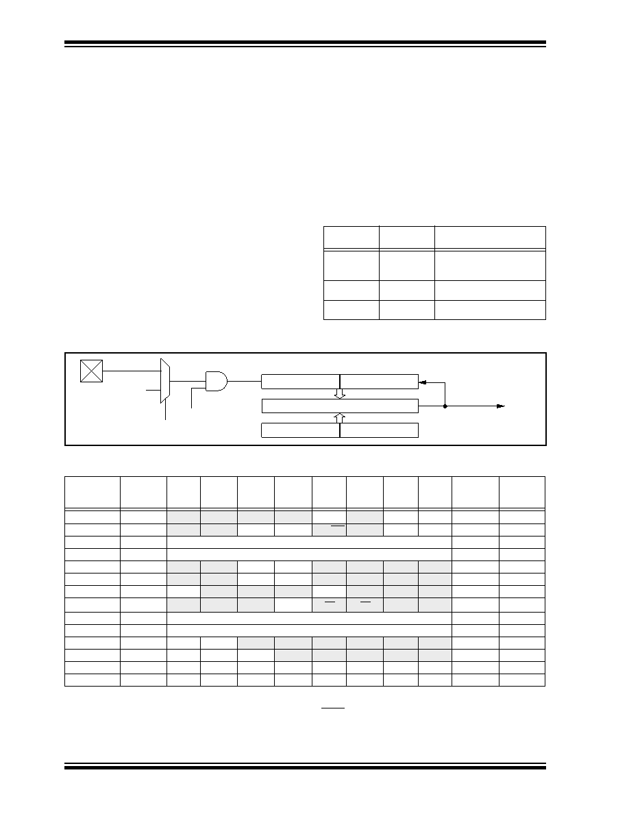
FIGURE 12-4: TMR1 AND TMR2 IN 16-BIT TIMER/COUNTER MODE
TABLE 12-2:
SUMMARY OF TIMER1 AND TIMER2 REGISTERS
Address
Name
Bit 7
Bit 6
Bit 5
Bit 4
Bit 3
Bit 2
Bit 1
Bit 0
Value on
Power-on
Reset
Value on all
other resets
(Note1)
16h, Bank 3
TCON1
CA2ED1
CA2ED0
CA1ED1
CA1ED0
T16
TMR3CS TMR2CS TMR1CS 0000 0000
0000 0000
17h, Bank 3
TCON2
CA2OVF
CA1OVF PWM2ON PWM1ON CA1/PR3 TMR3ON TMR2ON TMR1ON 0000 0000
0000 0000
10h, Bank 2
TMR1
Timer1 register
xxxx xxxx
uuuu uuuu
11h, Bank 2
TMR2
Timer2 register
xxxx xxxx
uuuu uuuu
16h, Bank 1
PIR
RBIF
TMR3IF
TMR2IF
TMR1IF
CA2IF
CA1IF
TXIF
RCIF
0000 0010
17h, Bank 1
PIE
RBIE
TMR3IE
TMR2IE
TMR1IE
CA2IE
CA1IE
TXIE
RCIE
0000 0000
07h, Unbanked
INTSTA
PEIF
T0CKIF
T0IF
INTF
PEIE
T0CKIE
T0IE
INTE
0000 0000
06h, Unbanked
CPUSTA
—
STKAV
GLINTD
TO
PD
—
--11 11--
--11 qq--
14h, Bank 2
PR1
Timer1 period register
xxxx xxxx
uuuu uuuu
15h, Bank 2
PR2
Timer2 period register
xxxx xxxx
uuuu uuuu
10h, Bank 3
PW1DCL
DC1
DC0
—
xx-- ----
uu-- ----
11h, Bank 3
PW2DCL
DC1
DC0
TM2PW2
—
xx0- ----
uu0- ----
12h, Bank 3
PW1DCH
DC9
DC8
DC7
DC6
DC5
DC4
DC3
DC2
xxxx xxxx
uuuu uuuu
13h, Bank 3
PW2DCH
DC9
DC8
DC7
DC6
DC5
DC4
DC3
DC2
xxxx xxxx
uuuu uuuu
Legend: x = unknown, u = unchanged, - = unimplemented read as a '0', q - value depends on condition,
shaded cells are not used by Timer1 or Timer2.
Note 1:
Other (non power-up) resets include: external reset through MCLR and WDT Timer Reset.
RB4/TCLK12
Fosc/4
TMR1ON
(TCON2<0>)
TMR1CS
(TCON1<0>)
TMR1 x 8
PR1 x 8
Reset
Equal
Set Interrupt TMR1IF
(PIR<4>)
1
0
Comparator<8>
Comparator x16
TMR2 x 8
PR2 x 8
发布紧急采购,3分钟左右您将得到回复。
相关PDF资料
PIC24HJ256GP210-I/PT
IC PIC MCU FLASH 128KX16 100TQFP
PIC24HJ128GP310A-I/PF
IC PIC MCU FLASH 128KB 100-TQFP
DSPIC33FJ128GP310-I/PF
IC DSPIC MCU/DSP 128K 100TQFP
PIC16C66-20I/SO
IC MCU OTP 8KX14 PWM 28SOIC
DSPIC33FJ128MC510-I/PT
IC DSPIC MCU/DSP 128K 100TQFP
PIC16C66-20I/SP
IC MCU OTP 8KX14 PWM 28DIP
PIC18LF2620-I/SP
IC MCU FLASH 32KX16 28SDIP
PIC16F877-04I/P
IC MCU FLASH 8KX14 EE 40DIP
相关代理商/技术参数
PIC18F4620-I/P
功能描述:8位微控制器 -MCU 64KB 3968 RAM 36 I/O RoHS:否 制造商:Silicon Labs 核心:8051 处理器系列:C8051F39x 数据总线宽度:8 bit 最大时钟频率:50 MHz 程序存储器大小:16 KB 数据 RAM 大小:1 KB 片上 ADC:Yes 工作电源电压:1.8 V to 3.6 V 工作温度范围:- 40 C to + 105 C 封装 / 箱体:QFN-20 安装风格:SMD/SMT
PIC18F4620-I/P
制造商:Microchip Technology Inc 功能描述:IC 8BIT FLASH MCU 18F4620 DIP40
PIC18F4620-I/PT
功能描述:8位微控制器 -MCU 64KB 3968 RAM 36 I/O RoHS:否 制造商:Silicon Labs 核心:8051 处理器系列:C8051F39x 数据总线宽度:8 bit 最大时钟频率:50 MHz 程序存储器大小:16 KB 数据 RAM 大小:1 KB 片上 ADC:Yes 工作电源电压:1.8 V to 3.6 V 工作温度范围:- 40 C to + 105 C 封装 / 箱体:QFN-20 安装风格:SMD/SMT
PIC18F4620-I/PT
制造商:Microchip Technology Inc 功能描述:IC 8BIT FLASH MCU 18F4620 TQFP44
PIC18F4620T-I/ML
功能描述:8位微控制器 -MCU 64KB 3968 RAM 36 I/O RoHS:否 制造商:Silicon Labs 核心:8051 处理器系列:C8051F39x 数据总线宽度:8 bit 最大时钟频率:50 MHz 程序存储器大小:16 KB 数据 RAM 大小:1 KB 片上 ADC:Yes 工作电源电压:1.8 V to 3.6 V 工作温度范围:- 40 C to + 105 C 封装 / 箱体:QFN-20 安装风格:SMD/SMT
PIC18F4620T-I/PT
功能描述:8位微控制器 -MCU 64KB 3968 RAM 36 I/O RoHS:否 制造商:Silicon Labs 核心:8051 处理器系列:C8051F39x 数据总线宽度:8 bit 最大时钟频率:50 MHz 程序存储器大小:16 KB 数据 RAM 大小:1 KB 片上 ADC:Yes 工作电源电压:1.8 V to 3.6 V 工作温度范围:- 40 C to + 105 C 封装 / 箱体:QFN-20 安装风格:SMD/SMT
PIC18F4680-E/ML
功能描述:8位微控制器 -MCU 64KB 3328 RAM w/ECAN RoHS:否 制造商:Silicon Labs 核心:8051 处理器系列:C8051F39x 数据总线宽度:8 bit 最大时钟频率:50 MHz 程序存储器大小:16 KB 数据 RAM 大小:1 KB 片上 ADC:Yes 工作电源电压:1.8 V to 3.6 V 工作温度范围:- 40 C to + 105 C 封装 / 箱体:QFN-20 安装风格:SMD/SMT
PIC18F4680-E/P
功能描述:8位微控制器 -MCU 64KB 3328 RAM w/ECAN RoHS:否 制造商:Silicon Labs 核心:8051 处理器系列:C8051F39x 数据总线宽度:8 bit 最大时钟频率:50 MHz 程序存储器大小:16 KB 数据 RAM 大小:1 KB 片上 ADC:Yes 工作电源电压:1.8 V to 3.6 V 工作温度范围:- 40 C to + 105 C 封装 / 箱体:QFN-20 安装风格:SMD/SMT